

Inquire
1.What are the challenges in designing common-mode inductors for millimeter-wave devices?
Answer: Common-mode inductor design for millimeter-wave devices (frequencies typically above 30 GHz) faces multiple challenges.
Parasitic parameters dominate: At high frequencies, the parasitic capacitance (between wires and between wires and ground) and parasitic inductance (from leads) of the windings have a significant impact, causing the actual impedance to deviate from the designed value and significantly reducing filtering effectiveness.
Core material limitations: The magnetic permeability of traditional ferrite cores drops sharply at millimeter-wave frequencies (the core cutoff frequency is far below millimeter-wave frequencies), resulting in a surge in magnetic losses (eddy current and hysteresis losses), making it difficult to effectively increase inductance.
Size and integration conflicts: Millimeter-wave devices are often miniaturized, requiring miniaturization of common-mode inductors. However, the skin effect and proximity effect of the windings intensify with increasing frequency, leading to increased wire resistance and losses. This necessitates extremely fine wires or specialized winding processes (such as spiral or planar windings).
Electromagnetic radiation interference: At high frequencies, the common-mode inductor itself can become a radiation source, interfering with sensitive circuitry within the device. Therefore, a shielding structure must be designed to further reduce space.
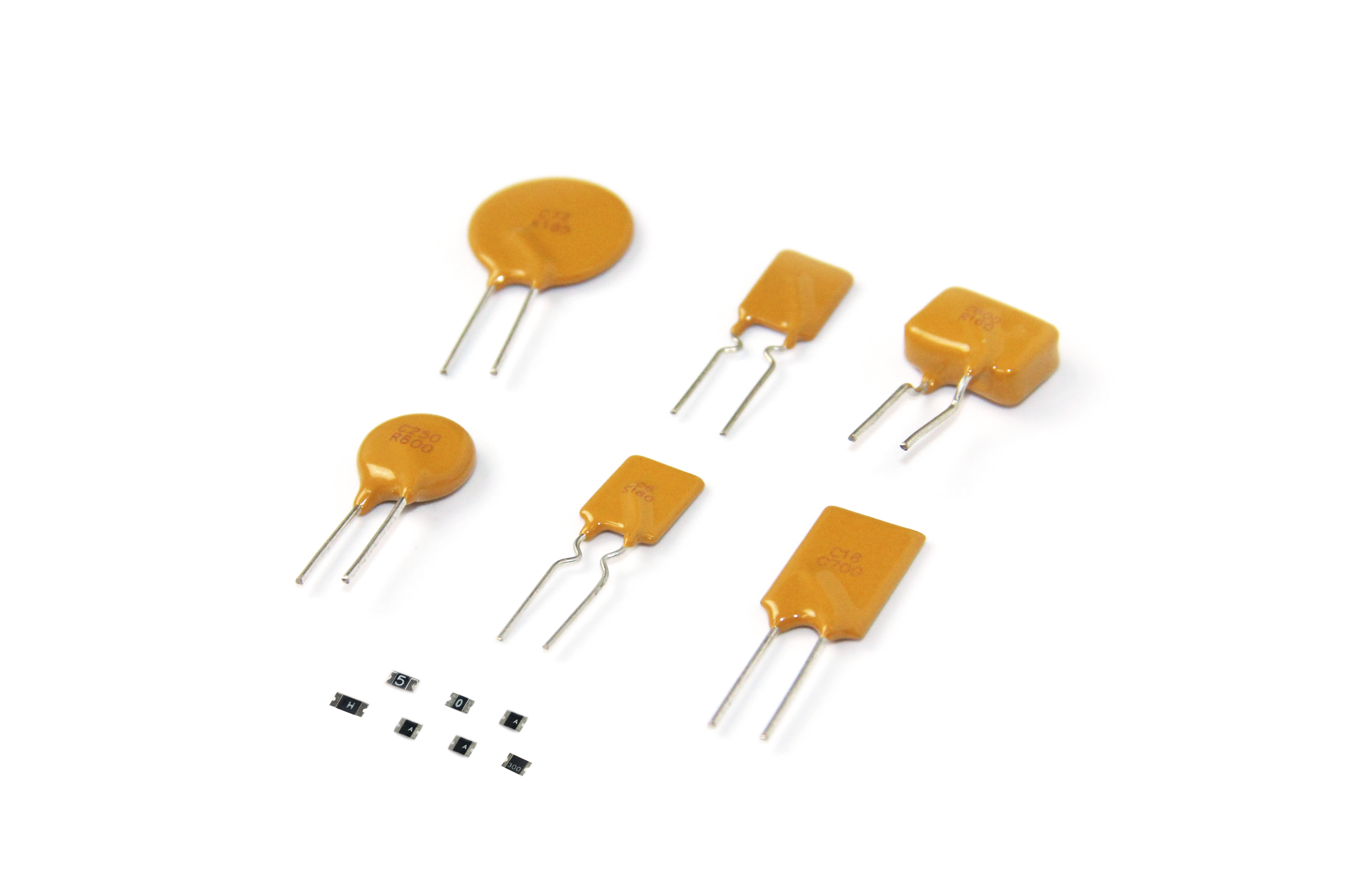
2. What are the material options for flexible common-mode inductors in flexible electronic devices?
Answer: Flexible electronic devices require common-mode inductors to maintain stable performance when bent and folded. Material selection must balance flexibility, magnetism, and conductivity:
Core Materials
Flexible Composite Magnetic Materials: Ferrite powder (such as Ni-Zn ferrite) mixed with flexible polymers such as silicone rubber and polyimide to achieve both magnetic and bendable properties.
Nanocrystalline Ribbons: Thinned (<10μm thick) nanocrystalline alloys (such as Fe-Si-B-Nb-Cu) are composited with flexible substrates (such as PET) to maintain high magnetic permeability while improving flexibility.
Winding Materials
Flexible Conductors: Ultra-thin copper foil (<5μm thick), silver-based conductive ink (printed on a flexible substrate), or metal braid (such as silver-plated copper wire) to ensure conductive continuity during bending.
Substrate / Packaging Materials: Polyimide (PI), polyethylene terephthalate (PET), and other polymers with good bending resistance and insulation properties serve as support for the windings and magnetic core.
3. Can traditional common-mode inductor structures be used to suppress common-mode interference in the terahertz band?
Answer: Not suitable. Traditional common-mode inductors rely on a magnetic core to enhance inductance, but this core principle fails in the terahertz frequency band (0.3-3 THz).
Core failure: The cutoff frequency of traditional magnetic cores (ferrite, nanocrystal) is far below terahertz (typically < 1 GHz), and their magnetic permeability approaches 1 (equivalent to air), making magnetic enhancement impossible and causing a sharp drop in inductance.
Parasitic parameter dominance: The parasitic capacitance of the winding and the lead inductance become the dominant parameters in the terahertz frequency band, resulting in uncontrollable impedance characteristics and ineffective common-mode interference suppression.
Alternative solutions: Filter structures based on transmission line theory (such as microstrip filters), photonic crystals, or metamaterial designs should be used to utilize the reflection/absorption properties of electromagnetic waves to suppress interference.
4. How can common-mode inductors in energy harvesting devices achieve a balance between low power consumption and high suppression?
Answer: Energy harvesting devices (such as photovoltaics and vibration power generation) consume extremely low power (in the μW range), and common-mode inductors must meet these requirements simultaneously.
Low-power design
Reduce winding losses: Use highly conductive materials (such as silver-plated copper wire) and thick conductors (to reduce DC resistance) to minimize skin effect (using stranded wire at high frequencies).
Reduce core losses: Select high-frequency, low-loss magnetic materials (such as low-loss ferrites and nanocrystalline ribbons) to avoid core saturation at the operating frequency (optimize core size and number of turns).
High suppression performance
Match the interference frequency band: Optimize inductance and parasitic capacitance through simulation to ensure high impedance at the target interference frequency (e.g., 100kHz-100MHz).
Miniaturization and parasitic control: Use planar windings (to reduce volume) and shorten lead lengths (to reduce parasitic inductance) to avoid additional losses.
Balanced strategy: Through the coordinated design of core materials and winding parameters (e.g., "low-loss core + appropriate inductance"), the power consumption of the device can be controlled to within 5% of the total device power consumption while meeting interference suppression requirements. Within
5. What are the application prospects of superconducting common-mode inductors in extreme environments?
Answer: Superconducting common-mode inductors (leveraging the zero-resistance property of superconducting materials) have unique advantages in extreme environments (low temperature, high radiation, and high vacuum). The prospects are as follows.
Application Scenarios
Aerospace Equipment: The low-temperature environment of space (such as satellites and deep space probes) can maintain a superconducting state, and their low loss characteristics make them suitable for long-term operation.
High-energy physics experiments: In high-radiation environments (such as particle colliders), superconducting materials offer superior radiation resistance compared to traditional conductors, resulting in higher reliability.
Deep-sea Equipment: In high-pressure, low-temperature environments, superconducting inductors can reduce heat dissipation pressure and are suitable for high-power transmission systems.
Challenges
Refrigeration Requirements: Most superconducting materials require low-temperature environments (such as liquid helium, which is 4K), making it difficult to maintain refrigeration systems in extreme environments. (High-temperature superconducting materials such as REBCO require liquid nitrogen at 77K, and thermal insulation is still required.)
Cost and Process: Superconducting materials (such as niobium titanium, REBCO) The cost of the strip material is high, and the winding process is complex (needing to avoid destruction of the superconducting state).
Prospects: In specific scenarios (such as naturally low-temperature environments without active cooling), superconducting common-mode inductors can significantly improve equipment efficiency and reliability. With the advancement of high-temperature superconducting materials, their application range will expand.
6. What are the design challenges of integrated common-mode inductors (integrated with capacitors and resistors)?
Answer: Integrated common-mode inductors (combining common-mode inductors with X/Y capacitors, resistors, etc.) face the following challenges:
Electromagnetic coupling interference: The magnetic field of the common-mode inductor may couple to adjacent capacitors/resistors, causing capacitance drift and increasing resistor noise, impacting filtering performance.
Parameter matching difficulties: After integration, parasitic parameters (such as the mutual inductance of the inductor and capacitors, and lead inductance) superimpose on each other, easily causing resonance point shifts. This requires repeated layout optimization through 3D simulation.
Heat dissipation issues: The densely packed components lead to heat concentration, impacting the performance of the magnetic core (permeability decreases at high temperatures) and the capacitors (temperature sensitivity). This requires the design of heat dissipation channels (such as metal substrates).
Process compatibility: The magnetic core manufacturing (such as sintering) and the capacitor/resistor process (such as thin film deposition) may conflict (e.g., high-temperature sintering damages the capacitor dielectric). This necessitates the development of hybrid processes (e.g., low-temperature curing magnetic material + thin-film components).
Debugging complexity: Adjusting individual component parameters can affect overall performance. Modular design (such as replaceable component units) is needed to reduce debugging difficulties.
7.3D What is the current status of 3D printing technology in the manufacture of common-mode inductor cores?
Answer: 3D printing technology is still in the exploratory stage in the manufacture of common-mode inductor cores. The current status is as follows:
Material Progress: Printable core materials have been developed, such as:
Ferrite powder + polymer binder (such as PLA) composites, which can be printed via fused deposition modeling (FDM) or stereolithography (SLA) with magnetic permeability approximately 30%-50% of that of traditional ferrite
Metallic magnetic powders (such as Fe-Co alloy) mixed with a binder, suitable for selective laser sintering (SLS), which can increase magnetic density but also has high losses.
Application Scenarios: Primarily used for prototyping and small-batch customization, such as special-shaped cores (asymmetric structures, internal openings to optimize the magnetic circuit), to quickly verify design solutions.
Limitations: o Performance Inadequacies: Printed cores have low density (porosity), lower permeability and saturation flux density than traditional sintered cores, and high high-frequency losses.
Efficiency and Cost: Slow printing speed (especially for complex structures), high material costs, and unsuitable for large-scale mass production.
Future Directions: Developing high-permeability printing materials (such as nanocomposite magnetic powders), optimizing the printing process (such as high-pressure forming to increase density), and expanding to small- and medium-batch customization scenarios.
8. How can self-diagnostic functions (such as temperature monitoring) be implemented in common-mode inductors?
Answer: The self-diagnostic function of a common-mode inductor (using temperature monitoring as an example) can be implemented through the following methods:
Sensor Integration
Built-in Temperature Sensor: Directly monitor the temperature by attaching an NTC thermistor, thin-film thermocouple, or printing temperature-sensitive conductive ink (such as carbon nanotube ink) to the core surface or near the windings.
Indirect Monitoring: Utilize the temperature characteristics of the winding resistance (copper's resistance temperature coefficient is approximately 0.004/°C) to infer the temperature by measuring the change in the winding's DC resistance (RDC) (ΔT = (R measured - R room temperature) / R room temperature / 0.004).
Signal Transmission and Processing: Connect the sensor signal via leads to the device's main control circuit (such as an MCU), collect data in real time, and set thresholds (such as the core's maximum temperature tolerance). 125°C). Exceeding this limit triggers an alarm (e.g., power off, indicator light).
Extended Function: Combined with impedance monitoring (using a network analyzer or built-in circuitry to measure the impedance changes of the common-mode inductor), this function can identify issues such as core aging (decreased permeability) and winding short circuits (sudden impedance drop). This, combined with temperature monitoring, improves diagnostic accuracy.
9. What are the implementation methods for reconfigurable common-mode inductors (with adjustable parameters)?
Answer: Reconfigurable common-mode inductors adapt to different scenarios by dynamically adjusting parameters. Implementation methods include:
Core Control
External Magnetic Field Control: Using magnetostrictive materials (such as Terfenol-D) or tunable cores (such as ferrite + coil, where the magnetic bias is changed by controlling the coil current) to adjust the magnetic permeability and thus the inductance value.
Temperature Control: Using temperature-sensitive magnetic materials (such as some ferrites, whose magnetic permeability changes suddenly within a specific temperature range), the inductance can be switched by heating/cooling.
Winding Control
Tap Switching: Designing a winding with multiple taps, using relays or MOSFETs to switch between different turns, changes the inductance value (e.g., a turns ratio of 2:1, an inductance ratio of 4:1).
Coupling Control: Changing the coupling coefficient between the two windings through mechanical structures (such as sliding the winding position) adjusts the equivalent inductance.
Circuit-Assisted Control
Parallel Variable Capacitor: Forming an LC network with the common-mode inductor, adjusting the capacitance value changes the resonant frequency, indirectly creating a "tunable inductor."
Semiconductor Bypass: Using MOSFETs By bypassing some windings or the core, the effective magnetic path length is changed, achieving continuously adjustable inductance.
10. What is the limit of miniaturization for common-mode inductors in biomedical implants?
Answer: The miniaturization of common-mode inductors for biomedical implantable devices (such as pacemakers and neurostimulators) is limited by multiple factors. The current limits are as follows:
Size range: Typically 0.5-2mm in diameter, 1-5mm in length (depending on the application).
Limiting factors:
Inductance requirement: At least several to tens of μH are required to suppress common-mode interference in the physiological signal frequency band (e.g., 0.1-10kHz). A small size (<0.5mm³) is difficult to achieve (core volume is positively correlated with inductance).
Winding and core material: The winding wire diameter must be ≥5μm (otherwise, the resistance is excessive, and losses exceed 10% of the device's total power consumption). The core must have sufficient volume (≥0.1mm³) to provide effective magnetic permeability.
Biocompatibility: The housing must be made of a biocompatible material (e.g., titanium alloy or ceramic) with a thickness of ≥50μm, further limiting the size of internal components.
Heat dissipation: Miniaturization increases thermal resistance, and temperature rise must be controlled within a certain range. Limit power density to within 0.5°C (to avoid damage to human tissue).
Future trends: Using nanomagnetic materials (such as magnetic nanoparticle composites) and three-dimensional windings (to improve space utilization) could potentially reduce the maximum size to 0.3mm in diameter and 0.8mm in length. However, this requires overcoming material and process bottlenecks.