|


| Quantity: | |
|---|---|
Specifications
Brand: YINT
Min. Order: 1 piece
Certification: RoHS
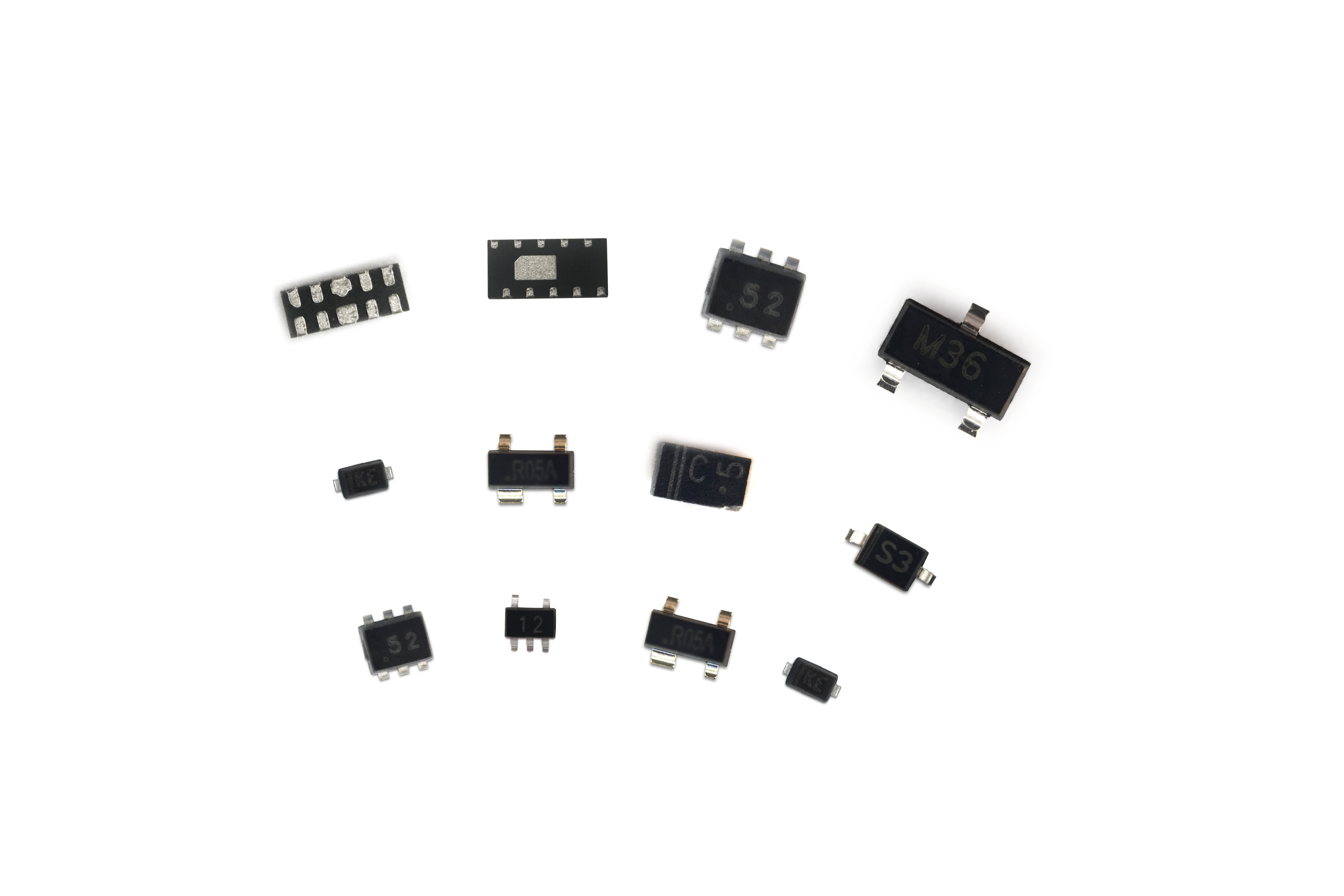
Packaging: in reel
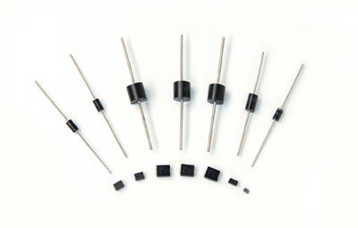
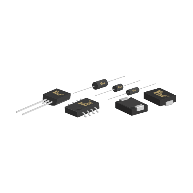
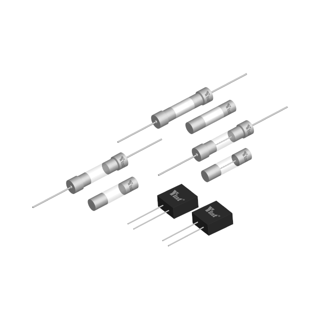
Bypass Diodes for Solar Panels
Maximum Junction Temperture 200℃
High Thermal Reliablity
Patented Super Barrier Rectifier Technology
High Forward Surge Capability
Ultra Low Power Loss,High Efficiency
Excellent High Temperature Stability
Maximum Ratings and Electrical Characteristics(TA=25℃ unless otherwise noted)
Single Phase,half wave,60HZ,resistive or inductive load.
For capacitive load,derate current by 20%
| Symbol | Parameter | Value | Unit |
| VRRM | Peak Repetitive Reverse Voltage | 45 | V |
| VRWM | Working Peak Reverse Voltage | ||
| VR | DC Blocking voltage | ||
| VR(RMS) | RMS Reverse Voltage | 32 | V |
| IO | Average Rectified Output Current(Note1)@TL=90℃ | 10.0 | A |
| IFSM | Non-repetitive Peak Forward Surge Current @ t=8.3ms Single half sine-wave superimposed on rated load (JEDEC Method) @TL=75℃ | 275 | A |
| VFM | Forword Voltage Drop @IF=8A,Tj=25℃ @IF=10A,Tj=25℃ @IF=10A,Tj=125℃ | 0.42 0.47 0.41 | V |
| IRM | Peak Reverse Curren @VF=45V, Tj=25℃ AT Rated DC Blocking Voltage @ VF=45V, Tj=100℃ @VF=45V,Tj=150℃ | 0.3 15 75 | mA |
| PARM | Repetitive Peak Avalanche Power(1us,25℃) | 30000 | W |
| RΘJA | Typical Thermal Resistance Junction to Ambient(Note2) (Note3) | 73 31 | ℃/W |
| Tj | Operting Temperature Range @VR≤80% VRRM @VR≤50% VRRM DC Forward mode | -65~+150 ≤180 ≤200 | ℃ |
| Tstg | Storage Temperature | -65~+150 | ℃ |
Note:
1.Valid provided that leads are kept at ambient temperature at a distance of 9.5mm from the case
2.FR-4 PCB,2OZ.Copper,minimum recommended pad layout
3.Polymide PCB,2OZ.Copper.Cathode pad dimensions 18.8mm*14.4mm.Anode pad dimensions 5.6mm*14.4mm
※ Disclaimer
Users should verify actual device performance in their specific applications.
Specifications are subject to change without notice.
The device characteristics and parameters in this data sheet can and do vary in different applications and actual device performance may vary over time.
Hot Tags: yint1045 to-277 schottky diode, China, manufacturers, factory, price, SMC Schottky Rectifiers, Schottky Rectifiers, SMD Schottky Barrier Diode, SMC Schottky Diode, Schottky Barrier Diode, Schottky Rectifier
Specifications
Brand: YINT
Min. Order: 1 piece
Certification: RoHS
Packaging: in reel
Bypass Diodes for Solar Panels
Maximum Junction Temperture 200℃
High Thermal Reliablity
Patented Super Barrier Rectifier Technology
High Forward Surge Capability
Ultra Low Power Loss,High Efficiency
Excellent High Temperature Stability
Maximum Ratings and Electrical Characteristics(TA=25℃ unless otherwise noted)
Single Phase,half wave,60HZ,resistive or inductive load.
For capacitive load,derate current by 20%
| Symbol | Parameter | Value | Unit |
| VRRM | Peak Repetitive Reverse Voltage | 45 | V |
| VRWM | Working Peak Reverse Voltage | ||
| VR | DC Blocking voltage | ||
| VR(RMS) | RMS Reverse Voltage | 32 | V |
| IO | Average Rectified Output Current(Note1)@TL=90℃ | 10.0 | A |
| IFSM | Non-repetitive Peak Forward Surge Current @ t=8.3ms Single half sine-wave superimposed on rated load (JEDEC Method) @TL=75℃ | 275 | A |
| VFM | Forword Voltage Drop @IF=8A,Tj=25℃ @IF=10A,Tj=25℃ @IF=10A,Tj=125℃ | 0.42 0.47 0.41 | V |
| IRM | Peak Reverse Curren @VF=45V, Tj=25℃ AT Rated DC Blocking Voltage @ VF=45V, Tj=100℃ @VF=45V,Tj=150℃ | 0.3 15 75 | mA |
| PARM | Repetitive Peak Avalanche Power(1us,25℃) | 30000 | W |
| RΘJA | Typical Thermal Resistance Junction to Ambient(Note2) (Note3) | 73 31 | ℃/W |
| Tj | Operting Temperature Range @VR≤80% VRRM @VR≤50% VRRM DC Forward mode | -65~+150 ≤180 ≤200 | ℃ |
| Tstg | Storage Temperature | -65~+150 | ℃ |
Note:
1.Valid provided that leads are kept at ambient temperature at a distance of 9.5mm from the case
2.FR-4 PCB,2OZ.Copper,minimum recommended pad layout
3.Polymide PCB,2OZ.Copper.Cathode pad dimensions 18.8mm*14.4mm.Anode pad dimensions 5.6mm*14.4mm
※ Disclaimer
Users should verify actual device performance in their specific applications.
Specifications are subject to change without notice.
The device characteristics and parameters in this data sheet can and do vary in different applications and actual device performance may vary over time.
Hot Tags: yint1045 to-277 schottky diode, China, manufacturers, factory, price, SMC Schottky Rectifiers, Schottky Rectifiers, SMD Schottky Barrier Diode, SMC Schottky Diode, Schottky Barrier Diode, Schottky Rectifier