
 Global


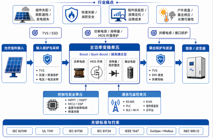
The optimizer is first and foremost a revenue-generating hardware that enhances component-level safety, component-level monitoring, compatibility with diverse inverters, component-level DC-DC conversion, MPPT/MSPT control, rapid shutdown/safety control, communication links, and integration with system-level monitoring platforms.
2.1 IEC 62109-1: General safety requirements for power conversion equipment used in photovoltaic systems. The IEC official description states that it applies to PCEs used in photovoltaic systems, covering basic safety requirements such as electric shock prevention, fire protection, and mechanical safety. IEC 62109-2: Further requirements for equipment with inverter functions or related power conversion functions.
2.2 UL1741: The North American market is important; UL indicates it applies to distributed energy resources. IEC 61730-1/61730-2: The IEC officially states that these two parts cover the construction requirements and testing requirements for photovoltaic modules, respectively. NEC 690.12 is a key source of requirements for rapid shutdown of rooftop photovoltaic systems in the United States.
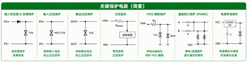
Shading, module mismatch, and power generation losses caused by module differences: under traditional string architecture, a single abnormal module can drag down the entire string's revenue. How to ensure safety in high-voltage DC rooftop systems: in traditional systems, fault localization is coarse, making it difficult to quickly identify module-level issues, leading to low operation and maintenance efficiency. A fundamental pain point in the optimizer industry is that as functionality increases, the number of components, connectors, and failure points also increases. EMI/EMC challenges are rising: after the superposition of power conversion, rapid shutdown, and communication monitoring, EMC difficulty has significantly increased.
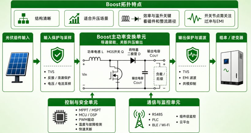
| Device Position | Functional Role | Yinte Can Provide |
|---|---|---|
| Inductor L | Energy storage, determines ripple and dynamic response | Power inductor |
| MOS | Switching control | MOS and gate protection |
| Diode / Rectifier | Freewheeling, output energy transfer | Schottky |
| Input protection position | Absorbs component-side transients | TVS |
| Switching node | Overshoot and EMI concentration point | TVS / Snubber / EMC |
| Output side | Output abnormality and surge risk | TVS |
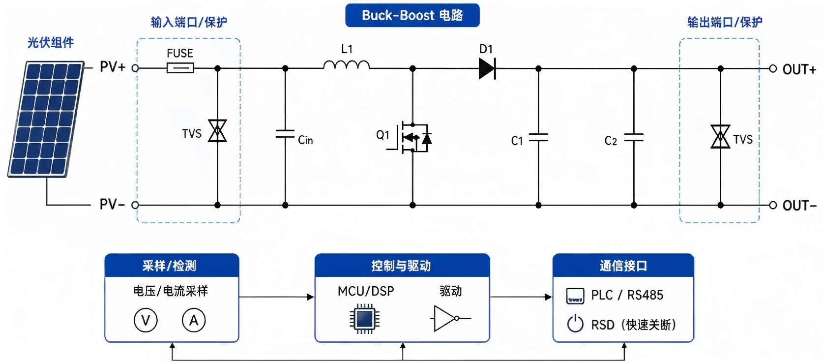
Buck-Boost is more suitable for real component scenarios, as it can accommodate both step-up and step-down operating conditions.
| Device Position | Functional Role | Yinte Can Provide |
|---|---|---|
| Main power inductor | Energy storage, maintains buck-boost conversion | Power inductor |
| Multiple MOSFETs | Form buck-boost switching network | MOSFETs and gate protection |
| Rectification/freewheeling path | Reduces loss, ensures continuous current | Schottky or synchronous rectification related |
| Input/output protection position | Absorbs surge and anomalies | TVS |
| High-frequency loop | EMI hotspot | Common-mode/filtering/absorption devices |
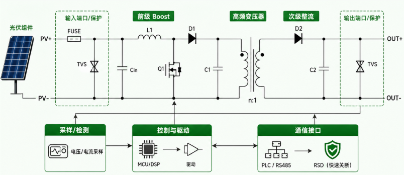
| Device Position | Functional Role | Yinte Can Provide |
|---|---|---|
| Coupling Inductor / Transformer | Core magnetic component | Magnetic component opportunity |
| Main Switch MOSFET | Primary-side energy control | MOSFET and protection |
| Secondary-side Rectification Path | Output rectification / freewheeling | Schottky / rectifier devices |
| Leakage Inductance Snubber Position | Suppress voltage spikes and overshoot | TVS / snubber network |
| Input / Output Protection Position | System protection | TVS |
| Common-mode Noise Path | EMC-sensitive position | Common-mode inductor / filter device |
| Dimension | Boost | Buck-Boost | Isolated/Coupled Type |
|---|---|---|---|
| Structural Complexity | Low | Medium-High | High |
| Operating Condition Adaptability | Medium | High | High |
| Component Count | Low | Medium | High |
| EMI Difficulty | Medium | Medium-High | High |
| Magnetic Component Requirement | Medium | Medium-High | High |
| Schottky Diode Opportunity | High | Medium-High | High |
| TVS Diode Opportunity | High | High | Very High |
| Inductor/Magnetic Component Opportunity | High | Very High | Very High |
| Application Location | Recommended Model | Suitability Judgment | Remarks |
|---|---|---|---|
| PV Input / 48V~60V Level Component Side Protection | NR5.0SMDJ75CA | Suitable as the first candidate for 48V~60V level systems | Suitable for initial Boost input prototype comparison |
| PV Input / 60V~80V Boundary More Conservative Solution | NR5.0SMDJ78CA | One step up from 75CA, suitable for candidates requiring higher margin | Can be verified in parallel with 75CA for comparison |
| Boost Output / 90V Level Bus Protection | NR5.0SMDJ90CA | Suitable for Boost output raised to approximately 90V level bus candidate | Suitable as one of the primary choices for output protection |
| Buck-Boost / Isolated Output / 110V~120V Level Protection | NR5.0SMDJ110CA | Suitable for higher output bus or 120V level chip and bus protection candidate | Suitable for use on the higher voltage output side |
Recommendation: For the single-block component side, non-isolated Boost input, you can first select one from the NR5.0SMDJ75CA / NR5.0SMDJ78CA for prototype comparison; for the Boost output, you can first consider the NR5.0SMDJ90CA; for the isolated/coupled type with higher output, you can first look at the NR5.0SMDJ110CA.
| Application Location | Recommended Model | Suitability Judgment | Remarks |
|---|---|---|---|
| Output Side 24V Auxiliary Power Supply | SMDJ24CA / 1.5KE35CA | Suitable for auxiliary power supply or 24V control branch | More suitable for control/communication branch |
| Output Side 5V Auxiliary Power Supply | SMBJ6.0CA | Suitable for 5V power supply port surge protection | Can be used with LDO/DC-DC input |
| Output Side 3.3V Logic Power Supply | ESD3V3D3B | Suitable for 3.3V low-voltage rail protection | Suitable for MCU/sampling/low-voltage logic power supply |
| 5V Low-Voltage ESD Protection | ESD5V0D3B | Suitable for 5V low-voltage ESD/hot-plug protection | Suitable for debug ports, auxiliary interfaces, and small power branches |
| Application Location | Recommended Model | Applicability Judgment | Remarks |
|---|---|---|---|
| RS485 Differential Port TVS | ESDSM712 | Primary protection device for RS485, high priority | Recommended to be placed near the interface side |
| RS485 Common-Mode Suppression | CML3225A-510T | Suitable as a candidate for communication link common-mode suppression | Used to suppress common-mode interference from long cables |
| RS485 Enhanced Overcurrent Protection | PPTC SMD1812-010-60V | Can be added for outdoor or long-cable environments | Enhances self-recovery capability after abnormal wiring and surges |
Recommended combination: ESDSM712 + CML3225A-510T + PPTC SMD1812-010-60V, suitable for initial prototyping of the optimizer communication system.
| Application Location | Recommended Model | Suitability Judgment | Remarks |
|---|---|---|---|
| Low-voltage signal line / debug port | ESD5V0D3B | General-purpose and reliable, suitable for 5V-class small-signal interfaces | Suitable for MCU debug port, low-speed IO |
| Higher-speed / low-capacitance interface | NRESDLLC5V0D25B | Suitable for interfaces prioritizing low capacitance | Suitable for monitoring / high-speed signal side |
| 5V multi-line interface | ESDSRVLC05-4 | Suitable for multi-line interface protection | Suitable for multi-line small-signal or data interfaces |
| Device Category | Current Recommendation | Reason | Reference Value |
|---|---|---|---|
| Main Power Inductor | First screen by inductance value, Isat, Irms, DCR, and temperature rise | Existing rule base does not consolidate specific models by power level | Boost / Buck-Boost main power inductor library |
| Coupled Inductor / Transformer | First screen by turns ratio, leakage inductance, core, and temperature rise | Isolation/coupling type requires customization or specific screening based on power level | Coupled magnetic component / transformer library |
| Main Power MOSFET | First screen by Vds, Id, Rds(on), Qg, and thermal resistance | Rule base currently lacks a MOSFET model library segmented by topology/power range | High-voltage main power MOSFET library |
| MOSFET Gate Protection Device | First design by gate resistor + Zener/TVS + snubber network | No specific gate protection device models have been accumulated yet | MOSFET gate protection dedicated component library |
 Hot News


 沪公网安备31011702889749号

